- 您现在的位置:买卖IC网 > Sheet目录1223 > KIT10XS3535EVBE (Freescale Semiconductor)KIT EVAL BOARD FOR 10XS3535
�� �
�
�FUNCTIONAL� DEVICE� OPERATION�
�PROTECTION� AND� DIAGNOSIS� FEATURES�
�EXTERNAL� PIN� STATUS�
�The� 10XS3535� provides� the� status� of� the� FLASHER,� FOG,�
�and� IGN� pins� via� the� SPI� in� real� time� and� in� Normal� mode.�
�FAILURE� HANDLING� STRATEGY�
�A� highly� sophisticated� failure� handling� strategy� enables�
�light� functionality� even� in� case� of� failures� inside� the�
�component� or� the� light� module.� Components� are� protected�
�against:�
�?� Reverse� Polarity�
�?� Loss� of� Supply� Lines�
�?� Fatal� Mistreatment� of� Logic� I/O� Pins�
�REVERSE� POLARITY� PROTECTION� ON� VBAT�
�In� case� of� a� permanently� reverse� polarity� operation,� the�
�output� transistors� are� turned� ON� (Rsd)� to� prevent� thermal�
�overloads� and� no� protections� are� available.�
�An� external� diode� on� VCC� is� necessary� in� order� to� not� to�
�destroy� the� 10XS3535� in� cases� of� reverse� polarity.�
�In� case� of� negative� transients� on� the� V� BAT� line� (per�
�ISO� 7637),� the� VCC� line� is� still� operating,� while� the� VBAT� line�
�is� negative.� Without� loads� on� OUT1:5� terminal,� an� external�
�clamp� between� V� BAT� and� GND� is� mandatory� to� avoid�
�exceeding� maximum� rating.� The� maximum� external� clamp�
�voltage� shall� be� between� the� reverse� battery� condition� and� ?�
�-20� V.�
�Therefore,� the� device� is� protected� against� latch-up� with� or�
�without� load� on� OUT� outputs.�
�LOSS� OF� SUPPLY� LINES�
�The� 10XS3535� is� protected� against� the� loss� of� any� supply�
�line.� The� detection� of� the� supply� line� failure� is� provided� inside�
�the� device� itself.�
�LOSS� OF� VBAT�
�During� an� under-voltage� of� V� BAT� (V� BATPOR1� <�
�V� BAT� <� V� BATUV� ),� the� outputs� [1-5]� are� switched� off�
�immediately.� No� current� path� from� VBAT� to� VCC.� The�
�external� MOSFET� (OUT6)� can� be� controlled� in� Normal� Mode�
�?� all� latched� faults� are� maintained� under� V� CC� in� nominal�
�conditions.� In� case� V� BAT� is� disconnected,� OUT[1:5]�
�outputs� are� OFF.� OUT6� output� state� depends� on� the�
�previous� SPI� configuration.� The� SPI� configuration,�
�reporting� (if� V� BAT� was� previously� in� the� nominal� voltage�
�range� for� at� least� 35� ?� sec),� and� daisy-chain� features� are�
�provided� for� RST� is� set� to� logic� [1].� The� SPI� pull-up� and�
�pull-down� current� resistors� are� available.� This� fault�
�condition� can� be� diagnosed� with� UVF� fault� in� OD13�
�reporting� bit.� The� previous� device� configuration� is�
�maintained.� No� current� is� conducted� from� V� CC� to� V� BAT� .�
�LOSS� OF� V� CC� (DIGITAL� LOGIC� SUPPLY� LINE)�
�During� loss� of� V� CC� (V� CC� <� V� CCUV� )� and� with� wake=1,� the�
�10XS3535� is� switched� automatically� into� Fail� mode� (no�
�deglich� time).� The� external� SMART� MOSFET� is� OFF.� All� SPI�
�registers� are� reset� and� must� be� reprogrammed� when� V� CC�
�goes� above� V� CCUV� .� The� device� will� transit� in� OFF� mode� if�
�VBAT� <� V� BATPOR2� .�
�LOSS� OF� V� CC� AND� VBAT�
�If� the� external� V� BAT� and� V� CC� supplies� are� disconnected� (or�
�not� within� specification:� (V� CC� and� V� BAT� )� <� V� BATPOR1� ),� all� SPI�
�register� contents� are� reset� with� default� values� corresponding�
�to� all� SPI� bits� are� set� to� logic� [0]� and� all� latched� faults� are� also�
�reset.�
�LOSS� OF� GROUND� (GND)�
�During� loss� of� ground,� the� 10XS3535� cannot� operate� the�
�loads� (the� outputs� (1:5)� are� switched� OFF),� but� is� not�
�destroyed� by� the� operating� condition.� Current� limit� resistors� in�
�the� digital� input� lines� protect� the� digital� supply� against�
�excessive� current� (1kohm� typical).� The� state� of� the� external�
�smart� power� switch� controlled� by� FETOUT� is� not� guaranteed,�
�and� the� state� of� external� smart� MOS� is� defined� with� an�
�external� termination� resistor.�
�FATAL� MISTREATMENT� OF� LOGIC� I� /� O� PINS�
�The� digital� I� /� Os� are� protected� against� fatal� mistreatment�
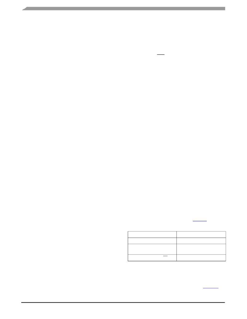
��Table� 16.� Logic� I� /� O� Plausibility� Check�
�by� the� SPI� if� VCC� remains� and� is� above� V� CCUV� .� The� fault� is�
�reported� to� the� UVF� bit� (OD13).� To� delatch� the� fault,� the�
�under-voltage� condition� should� be� removed� and:�
�?� To� turn-on� the� output,� the� corresponding� D7� bit� must� be�
�rewritten� to� logic� [1]� in� Normal� mode.� Application� of� the�
�OCHI� window� depends� on� toggling� or� not� toggling� the�
�D7� bit.�
�Input� /� Output�
�LIMP�
�(PWM)� CLOCK�
�SPI� (MOSI,� SCLK,� CS� )�
�Signal� Check� Strategy�
�Debounce� for� 10ms�
�Frequency� range�
�(bandpass� filter)�
�WD,� D10� bit� internal� toggle�
�?� If� the� device� was� in� Fail� mode,� the� fault� will� be� delatched�
�by� the� Autorestart� feature� periodically.�
�In� case� of� V� BAT� <� V� BATPOR1� (Power� OFF� mode),� the�
�behavior� depends� on� V� CC� :�
�?� all� latched� faults� are� reset� if� VCC� <� V� CCUV� ,�
�In� case� the� LIMP� input� is� set� to� logic� [1]� for� a� delay� longer�
�than� 10ms� typical,� the� 10XS3535� is� switched� into� Fail� mode.�
�In� case� of� a� (PWM)� Clock� failure,� no� PWM� feature� is� provided�
�and� the� bit� D7� defines� the� outputs� state.� In� case� of� SPI� failure,�
��MC10XS3535�
�Analog� Integrated� Circuit� Device� Data� ?�
�38�
�Freescale� Semiconductor�
�发布紧急采购,3分钟左右您将得到回复。
相关PDF资料
KIT13892VLEVBEJ
KIT EVAL FOR MC13892
KIT17C724EPEVBE
KIT FOR 17C7242CH HBRIDGE PWR IC
KIT33810EKEVME
BOARD EVAL FOR MC33810
KIT33811EGEVBE
KIT EVAL 33811 SOLENOID MON IC
KIT33812ECUEVME
KIT DESIGN FOR 33812/S12P
KIT33812EKEVBE
BOARD EVALUATION FOR MC33812
KIT33879AEKEVBE
BOARD EVALUATION FOR MC33879
KIT33880DWBEVB
KIT EVAL FOR MC33880 8X SW W/SPI
相关代理商/技术参数
KIT10XS4200EVBE
制造商:Freescale Semiconductor 功能描述:EVAL BOARD, MC10XS4200 HIGH SIDE SWITCH; Silicon Manufacturer:Freescale; Silicon Core Number:MC10XS4200; Kit Application Type:High Side Switch; Application Sub Type:-; Kit Contents:Eval Board MC10XS4200, CD ROM
KIT-1113C
制造商:ABIKO 功能描述:Bulk
KIT1116-400
制造商:Laird Technologies Inc 功能描述:ANTKIT,FG 128-137MHZ/ODB + FM2
KIT-113-175C
制造商:LG Corporation 功能描述:KIT TUNER 113-175C (113-175E +
KIT1133-P250
功能描述:ANTKIT GB8W15FT CABLE 制造商:laird technologies ias 系列:* 零件状态:在售 标准包装:1
KIT-11591
功能描述:ISP POGO ADAPTER KIT 制造商:sparkfun electronics 系列:- 零件状态:在售 套件类型:初级入门套件 主要用途:ISP Pogo 适配器 标准包装:1
KIT1167-120
制造商:Laird Technologies Inc 功能描述:ANT KIT GPS1575PW 20FT 制造商:Laird Technologies Inc 功能描述:ANTKIT,GPS1575PW/20FT
KIT1185-120
制造商:Laird Technologies Inc 功能描述:KIT ANT GPS 20FT 制造商:Laird Technologies Inc 功能描述:KIT1185-120